Polycrystalline thin-film growth
Polycrystalline thin-films are formed in a wide variety of thin-film deposition processes including chemical vapor deposition, physical vapor deposition, and sputter deposition.
A variety of models are being developed to study and simulate the evolution of the surface morphology and thin-film microstructure during growth. Both continuum and discrete models are being studied.
Topics of current interest include the effects of nucleation and substrate roughness on the average grain size and grain-size distribution, the effects of ion-erosion on facetting and on thin-film quality, and the development of improved mathematical methods for characterizing surface morphology.
Sputter deposition
Sputter deposition is a popular industrial process for rapid thin-film growth. Despite its importance in a variety of common industrial processes, including semiconductor chip manufacturing, the evolution of the surface morphology and microstructure during sputter deposition are poorly understood.
In sputter deposition, Ar ions collide with (i.e. "sputter") a target material, dislodging atoms which then travel back through the plasma and are deposited onto a substrate. While sputter deposition may lead to epitaxial growth, more commonly this process leads to polycrystalline thin-films.
The scattering of deposited atoms as they travel through the plasma leads to a range of angles over which atoms are deposited which may lead to a growth instability. We are studying the effects of this growth instability on the surface morphology and thin-film microstructure in all 3 zones of thin-film growth i.e. low-temperature, growth, intermediate temperature columnar growth, and high temperature "equi-axed" growth.
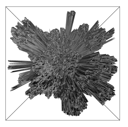
Simplified model of columnar growth studied by REU student Vera Verdree. (3D Projection - Top view)
Characterization of surface morphology in high-temperature sputter-deposition
Magnetron sputter deposition is being used at the University of Toledo by Prof. Compaan's group to deposit CdS/CdTe based solar cells. In collaboration with the Compaan group, and Prof. Arunan Nadarajah, who allowed us to use his atomic force microscope (AFM) REU student Ryan Snyder and I have studied the development of the surface morphology of CdS as a function of film thickness. Our results indicate the existence of an instability at early-times (small thicknesses) which is then partially stabilized by facetting as the growth proceeds. The morphology corresponds to high-temperature (zone III) equi-axed growth.
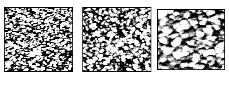
AFM scans (1 micron by 1 micron) od CdS sputter-deposited on glass at 250 C at different thicknesses (from left to right): 0.05 micron, 0.10 micron, and 0.2 micron.